Introduction
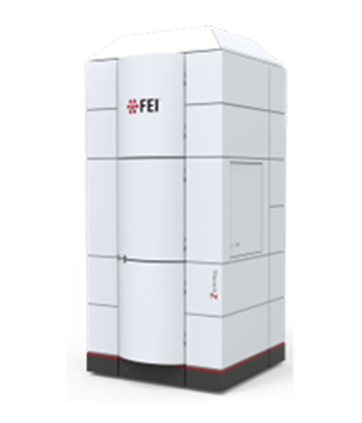
The field emission transmission electron microscope emits electrons with the field emission
electron emitter, and controls the electron beam to assemble into a small beam spot through the
electromagnetic lens and irradiate the sample. At the same time, the spherical aberration corrector is
used to eliminate the spherical aberration in the electromagnetic lens, which can improve the image
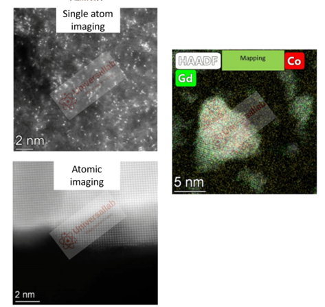
resolution and analysis ability to the atomic level, and realize the imaging and component analysis of
atomic resolution.
Technical specifications
1. Resolution: point resolution 0.11nm, line resolution 0.10nm, scanning transmission
image 0.08nm, transmission image 0.19nm.
2. Magnification: scanning transmission image 200 ~ 150,000,000x, transmission image 50
~ 2,000,000x.
3. Acceleration voltage: 80kV, 200kV.
4. Inclination Angle: X/Y maximum ±25°.
Application range
Test programs: TEM, STEM, EDS, Mapping, SAED, EELS.
ACTEM can be applied to do
1. Morphology observation: 2D microscopic morphological observation of the
microstructure of various materials, including powder, nanoparticle morphologies and particle size
observations; 3D stereoscopic morphologies can be obtained with 3D reconstruction.
2. - Structural analysis: use selected area electron diffraction, high-resolution
transmission images, high-resolution scanning transmission images, etc. to analyse the structure of
material.
3. - Component analysis: With the energy spectrometer, point, line, surface, and volume
distribution analysis of sample elements can be performed, and an atomic resolution element surface
distribution image can be obtained.
