Sample Requirement
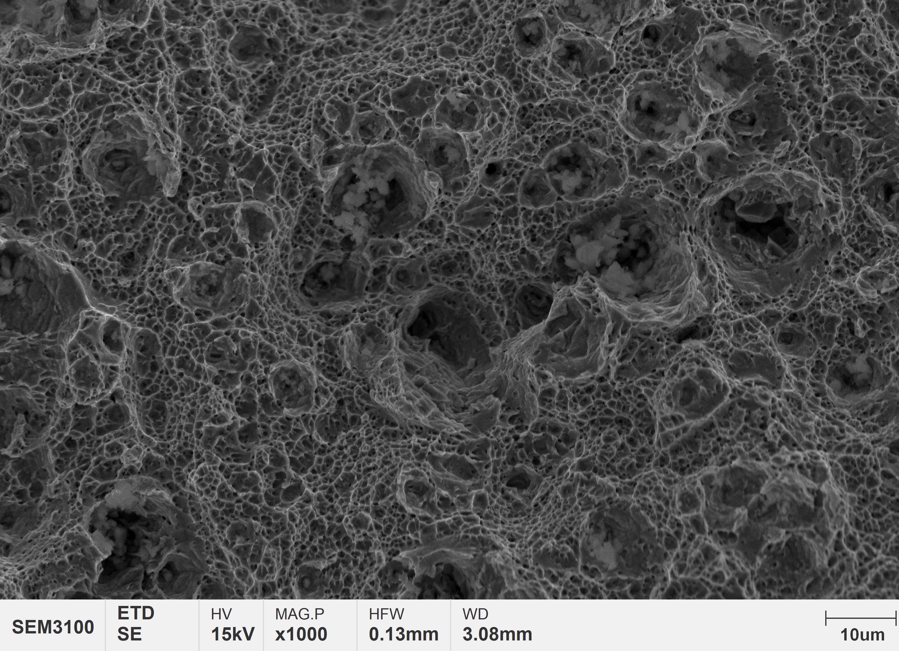
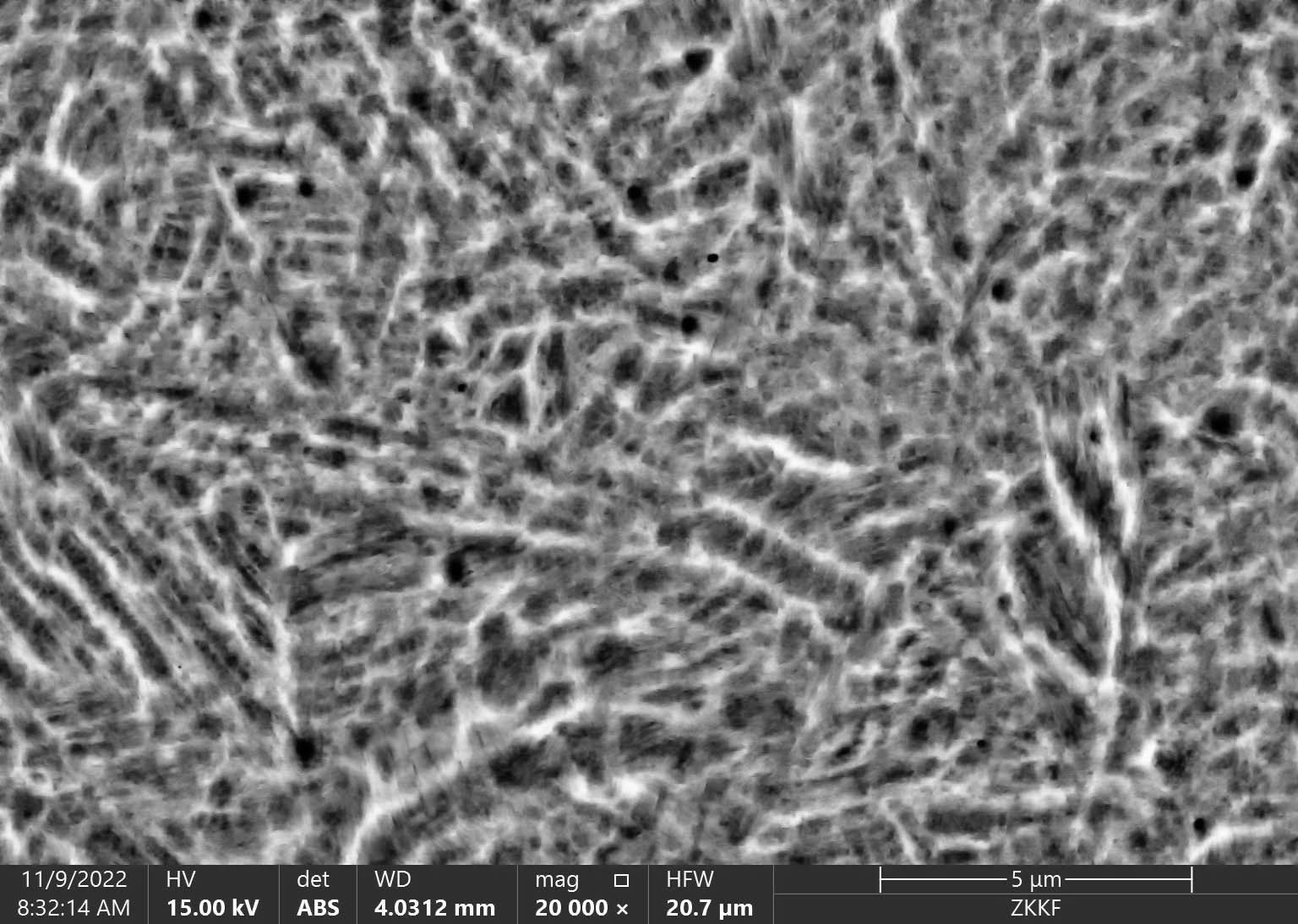
Samples for Scanning Electron Microscope (SEM) imaging must meet certain requirements
in order to obtain high-quality images. Here are some general requirements for preparing samples for SEM
imaging:
1. Size
Samples should be small enough to fit in the SEM chamber, which typically has a maximum
size limit of a few centimeters in diameter and a few centimeters in height. For ultra big sample,
please consult with us.
2. Conductivity
SEM requires that the sample is electrically conductive, or has been made conductive
through coating or other techniques, so that it can be grounded and imaged without charging. Materials
that are not inherently conductive, such as polymers or ceramics, may require a conductive coatingg,
such as gold or carbon.
3. Cleanliness
Samples should be free of debris and contaminants that could interfere with the imaging
process or damage the SEM equipment. Cleaning the sample with solvents or by other methods is usually
recommended.
4. Stability
Samples should be stable under the vacuum conditions inside the SEM chamber, which can
cause some materials to outgas or degrade.
5. Preparation
Samples should be prepared for SEM imaging according to the specific requirements of
the instrument and the application. This may involve coating the sample, cutting it to the appropriate
size, or applying a conductive paste to the edges to ensure good electrical contact.
Proper preparation of SEM samples is crucial for obtaining high-quality images and
accurate results. It is important to consult with the SEM manufacturer or an experienced SEM user for
guidance on sample preparation techniques for your specific application.
