Follow Us :

FIB TEM Sample Preparation

Instrument Type:

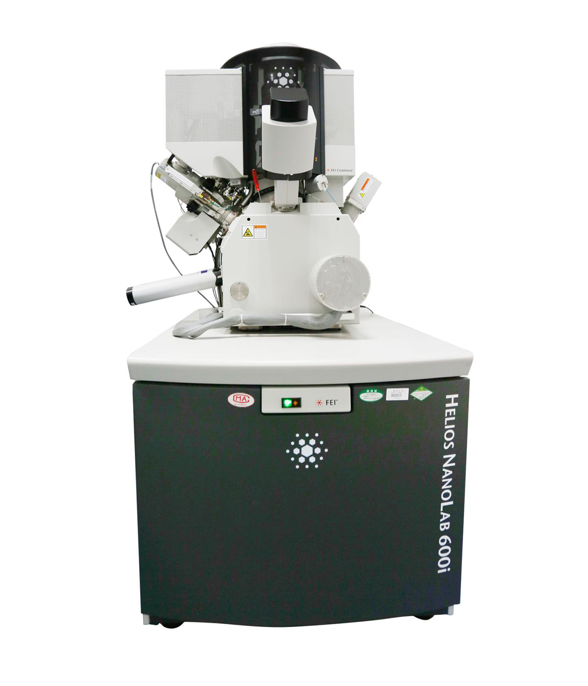
FEI Helios NanoLab 600i; ZEISS Crossbeam 540

Analytical Program:

Life-out: normal material -- 600 CHF/pillar

Life-out: ultra-hard/magnetic materials -- 800 CHF/pillar

Plan-view: normal material -- 800 CHF/pillar

Plan-view: ultra-hard/magnetic material -- 1000 CHF/pillar

Contact Us

Introduction

FIB (Focused Ion Beam) TEM (Transmission Electron Microscopy) Sample Preparation is a cutting-edge technique that allows for the preparation of extremely thin samples for high-resolution imaging and analysis with TEM. This technique uses a focused beam of ions to selectively remove material from a sample, allowing for precise and controlled preparation of samples for TEM imaging.

With FIB TEM Sample Preparation, researchers can gain unparalleled insights into the internal structure and composition of materials, including semiconductors, metals, ceramics, and biological specimens. This technique is particularly useful for analyzing complex and delicate samples, such as integrated circuits, nanomaterials, and biological tissues.

Our FIB TEM Sample Preparation service offers a complete solution for preparing samples for TEM analysis. Our experienced technicians use state-of-the-art equipment and techniques to produce high-quality, ultra-thin samples that are ideal for TEM imaging. We offer a range of sample preparation options, including cross-sectioning, site-specific milling, and TEM lamella preparation.
Representive Results

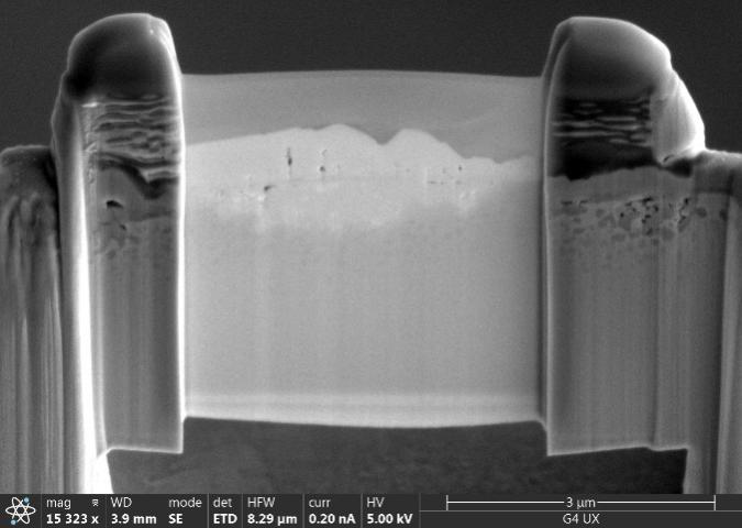
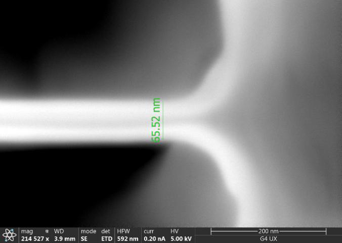
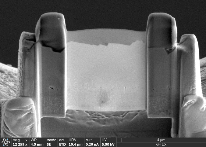
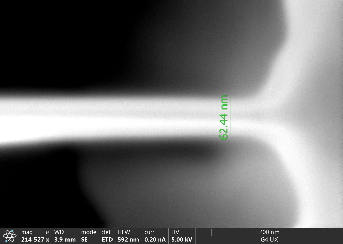
1. FIB TEM lamellar preparation for sample

Sample Requirement

1. Sample size

The sample should be small enough to fit into the FIB chamber, with blocks preferably less than 20 mm in length and width and less than 5 mm in heigh.

2. Sample shape

The sample should have a flat surface that can be mounted onthe FIB processing stand. Note that the sample may need to be cut or polished to obtain a flat surface

3. Sample material

The sample material should be compatible with FIB processing and typically includes metals, semiconductors, ceramics and biological samples. Samples should have good electrical conductivity or, if poorly conductive, should be coated with gold or carbon.

4. Sample thickness

The ideal sample thickness depends on the specific application and the type of analysis to be performed. In general, the sample thickness should be thin enough to allow electron transport in the TEM, typically less than 100 nm.

5. Sample quality

The sample should be of high quality with minimal defects or damage that could interfere with FIB processing or TEM imaging.

Related Products

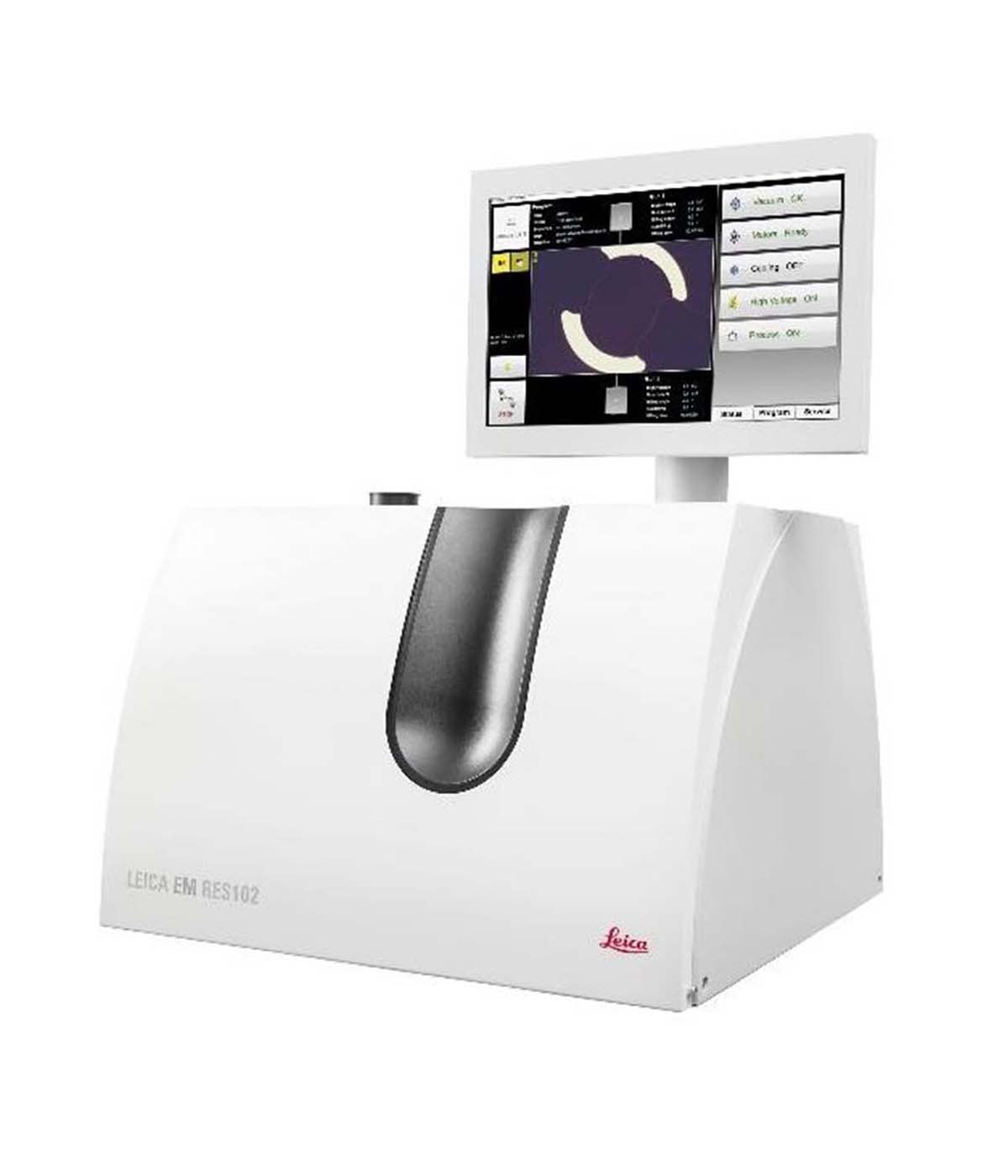
Ar lon Milling / Polishing

Reference price: from 200 CHF/sample

Read More
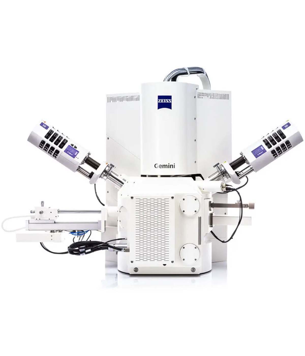
SEM Morphology Characterization

Reference price: from 80 CHF/sample

Read More
Surface Area and Porosity Analyzer BET

Reference price: from 20 CHF/sample

Read More
Ultraviolet/Visible/Near Infrared Spectroscopy

Reference price: from 50 CHF/sample

Read More