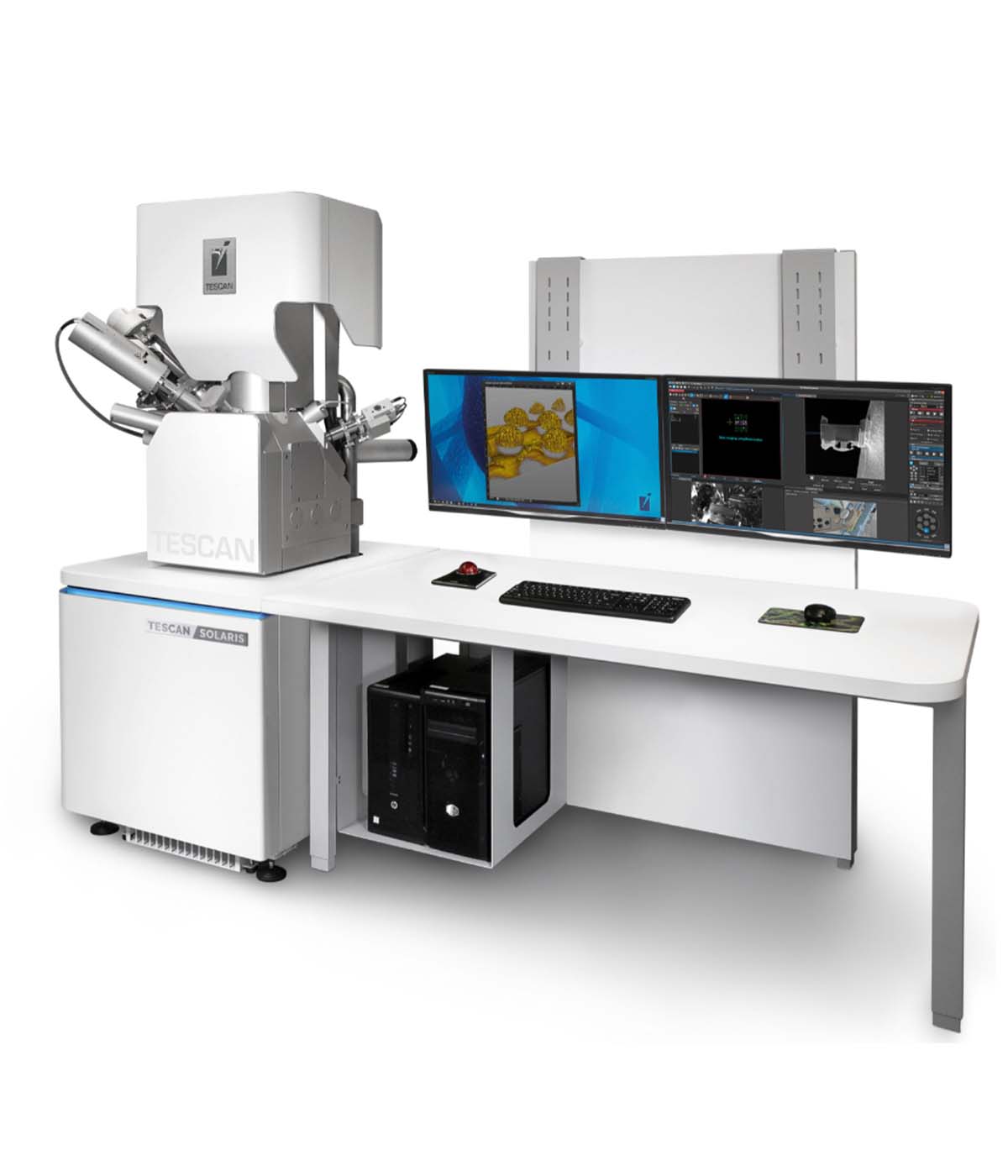
Electron Backscatter Diffraction (SEM EBSD)
Instrument Type:
EDAX TSL; Oxford Nordly max3
Analytical Program:
Mapping -- 80 CHF/map
Line scanning -- 50 CHF/line
Point analysis -- 30 CHF/ 3 point

Instrument Type:
EDAX TSL; Oxford Nordly max3
Analytical Program:
Mapping -- 80 CHF/map
Line scanning -- 50 CHF/line
Point analysis -- 30 CHF/ 3 point
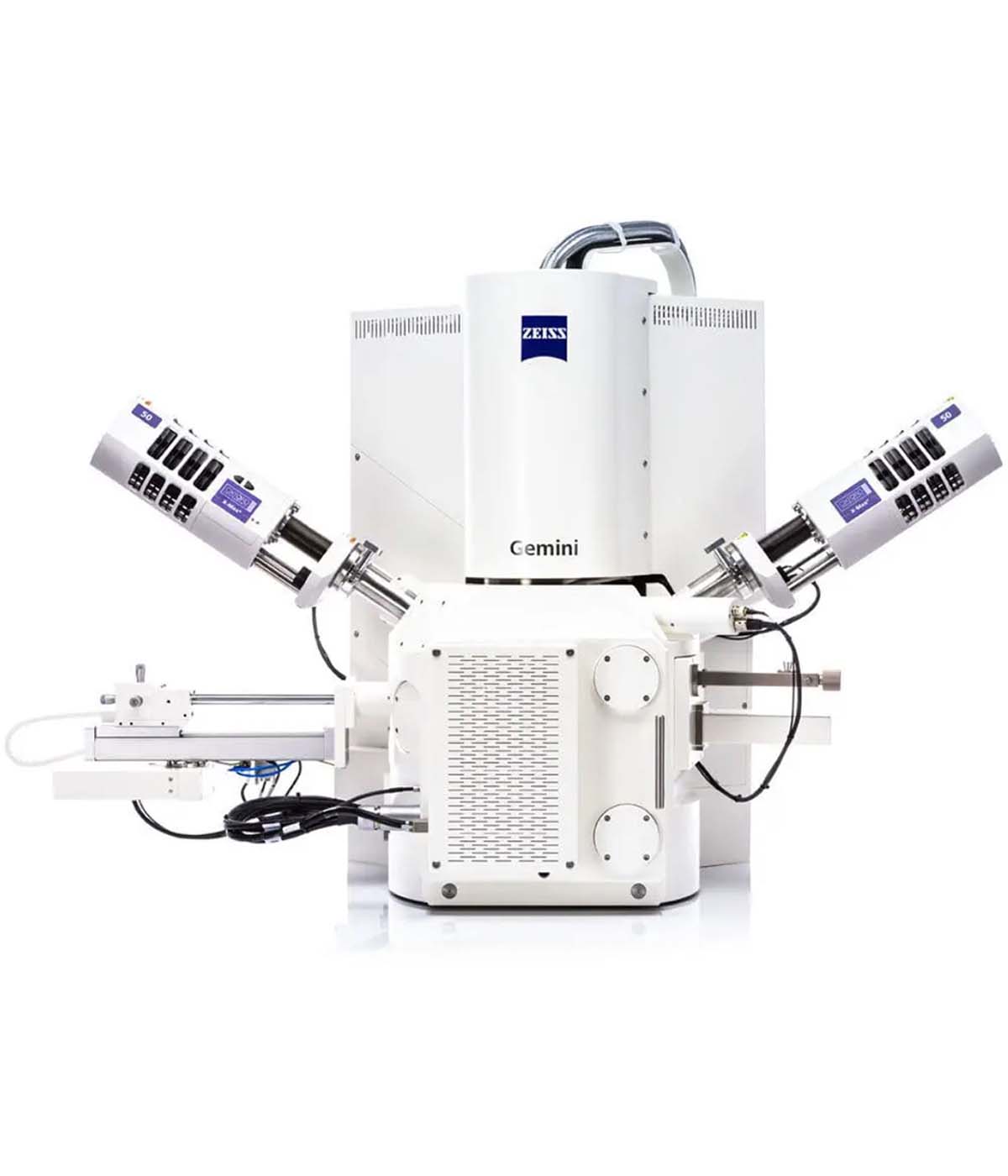
SEM EBSD is a technique used in materials science to study the crystallographic orientation of a sample using a scanning electron microscope. It provides information about the microstructure and mechanical properties of materials, particularly at the microscale, and is essential in materials science research and development.
SEM EBSD can be applied in:
(1) Rapid detection of orientation distribution.
(2) Orientation determination, such as single crystal, specific orientation grains, etc.
(3) Texture analysis.
(4) Geometrically necessary dislocation (GND) analysis.
(5) Recrystallization analysis.
(6) Calculation of plastic geometric factors (SF, TF).
(7) Preferred orientation analysis, such as PF, IPF, and ODF.
(8) Distribution of orientation difference.
(9) Graphical statistical analysis of grain size.
(10) Special grain boundary characterization.


To perform EBSD analysis, the sample should be flat, polished, clean, thin, and have a crystalline structure. The surface should be free of debris, scratches, or visible defects that can interfere with electron diffraction.
