Scanning Electron Microscope Electron Dispersive Spectroscopy (SEM EDS/EDX)
Instrument Type:
Analytical Program:
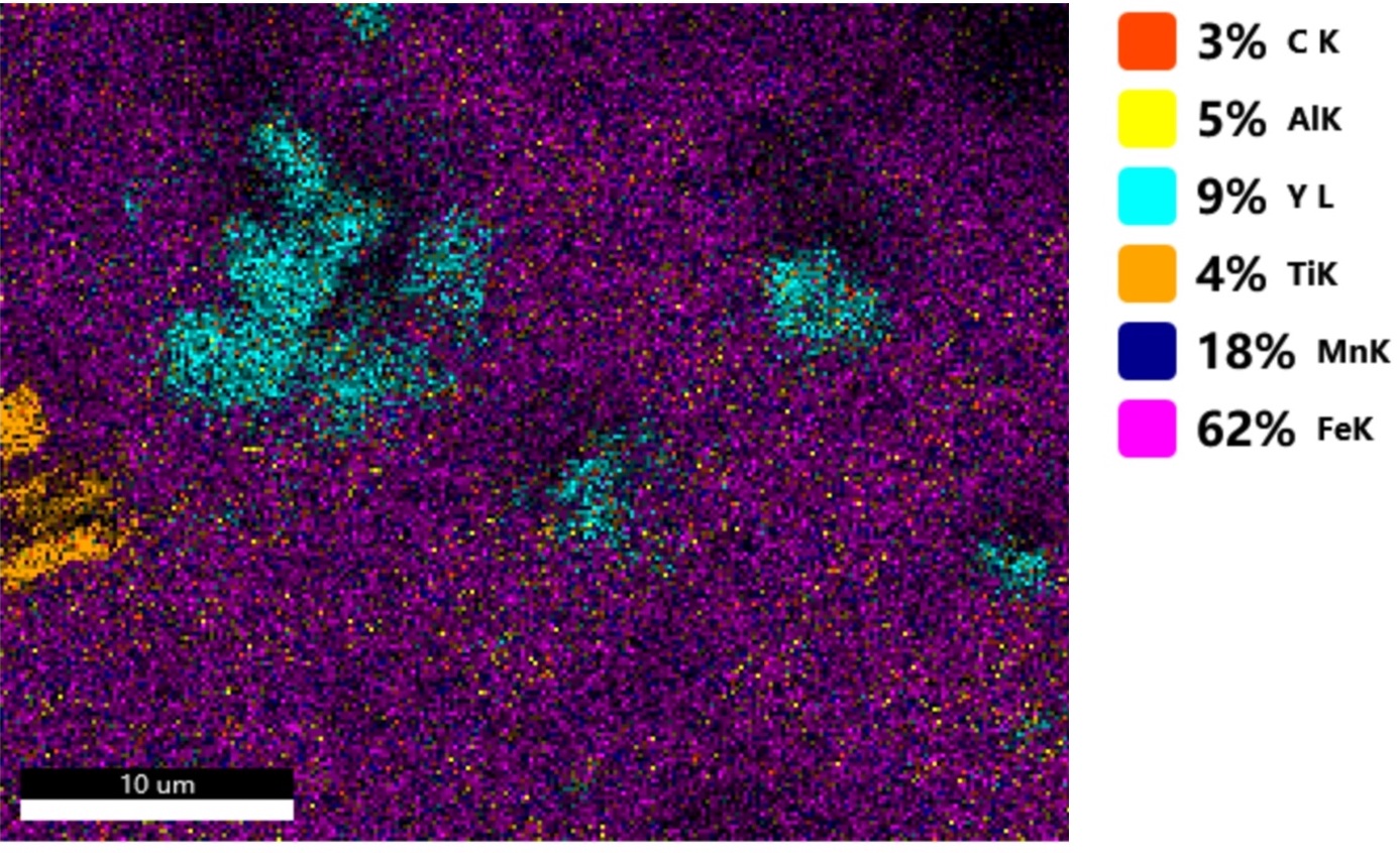
Mapping -- 80 CHF/map
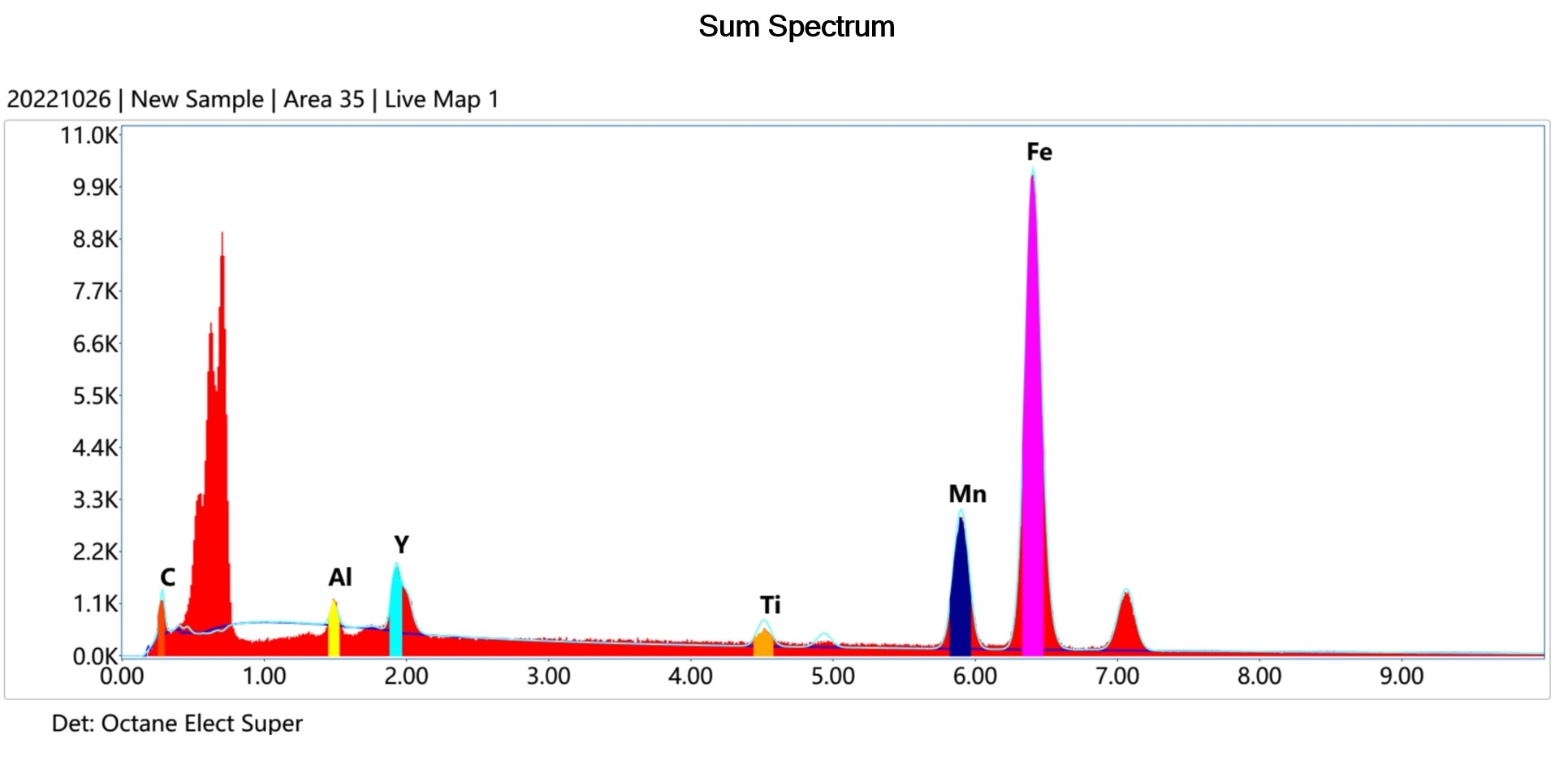
Line scanning -- 50 CHF/line
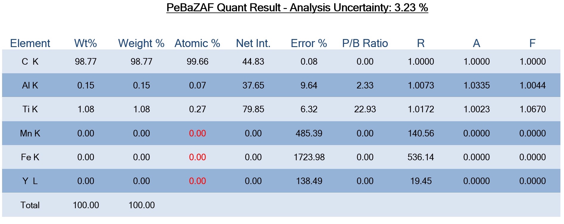
Point analysis -- 30 CHF/ 3 point

Instrument Type:
Analytical Program:
Mapping -- 80 CHF/map
Line scanning -- 50 CHF/line
Point analysis -- 30 CHF/ 3 point
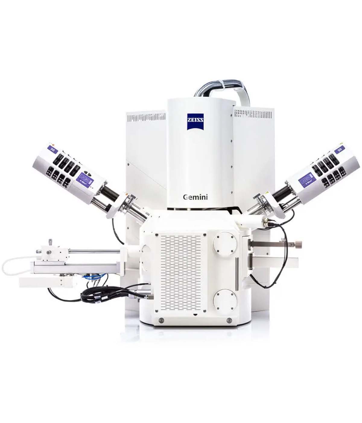
SEM EDS (Scanning Electron Microscope Energy Dispersive Spectroscopy) is an analytical technique that combines the high-resolution imaging capabilities of a scanning electron microscope (SEM) with the elemental analysis capabilities of energy dispersive X-ray spectroscopy (EDS).
It is used to obtain detailed information about the chemical composition of a sample at a micro- or nanoscale level.
SEM EDS is a non-destructive technique that can be used to analyze a wide range of materials and provides valuable information on the elemental composition, crystal structure, and chemical bonding of the sample.
Samples for SEM EDS must be completely dry to avoid interference from water and to prevent damage to the SEM instrument.
Samples must be clean and free of contaminants that may interfere with the analysis.
Samples must be small enough to fit into the SEM chamber and to be analysed by the electron beam. The size requirements depend on the specific SEM instrument being used and the nature of the sample.
Samples must be electrically conductive or coated with a conductive material to avoid charging and to produce clear images. Non-conductive samples may need to be coated with a conductive material such as gold or carbon.
